S-9.1 Electrical Standards
Original Version: 3/07/2020
Communication from a Digital Command Station to a Digital Decoder is accomplished by transmitting a series of bits that convey instructions. A bit is a signal which represents one of two conditions, which we will call 1 and 0. This portion of the standard covers the electrical characteristics of the digital command control signal that encodes these bits. Please refer to tables 1-32 for definition and numerical values of parameters used throughout this document.
A: Technique for Encoding Bits
The NMRA baseline digital command control signal consists of a stream of transitions between two equal voltage levels that have opposite polarity [1]. Alternate transitions separate one bit from the next. The remaining transitions divide each bit into a first part and a last part. Digital Command Stations shall encode bits within this digital command control stream of transitions by varying the duration of the parts of the bits, or frequency of the transitions.
In a 1 bit, the first and last part of a bit shall have the same nominal duration, and that duration shall be \(t_1\) [2], giving the bit a nominal total duration of \(2 \times t_1\). Digital Command Station components shall transmit 1 bits with the first and last parts each having a duration within the \(t_1\) range. The duration difference between the first and last parts of a 1 bit shall not exceed \(t_\mathrm{1d}\). A Digital Decoder must accept bits whose first and last parts have a duration within the \(t_\mathrm{r1}\) range as a valid bit with the value of 1. Digital Decoders must accept 1 bits where the duration difference between the positive and negative components does not exceed \(t_\mathrm{r1d}\).
In a 0 bit, the duration of the first and last parts of each transition shall nominally be greater than or equal to \(t_0\). To keep the DC component of the total signal at zero as with the 1 bits, the first and last part of the 0 bit are normally of equal duration. Digital Command Station components shall transmit 0 bits with each part of the bit having a duration within the \(t_0\) range with the total bit duration of the 0 bit not exceeding \(t_\mathrm{0total}\). A Digital Decoder must accept bits, whose first or last parts have a duration within the \(t_\mathrm{r0}\) range as a valid bit with the value of 0. Figure 1 provides an example of bits encoded using this technique.
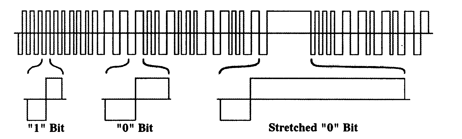
Figure 1: Bit Encoding
This is a differential signal with no ground. At the point where the signal line crosses the horizontal reference line, both rails will be at the same voltage.
One Bit Timing
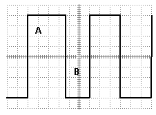
For power station output under load:
Relationship for One Bits |
Result |
|---|---|
\(t_\mathrm{A} \lt t_\mathrm{1min}\ \mathrm{or}\ t_\mathrm{A} \gt t_\mathrm{1max}\) |
Bad |
\(t_\mathrm{A} = t_\mathrm{B}\) |
OK |
\(t_\mathrm{A} - t_\mathrm{B}| \le t_\mathrm{1dmax}\) |
OK |
\(t_\mathrm{A} - t_\mathrm{B}| \gt t_\mathrm{1dmax}\) |
Bad |
Decoders must accept:
Relationship for One Bits |
Result |
|---|---|
\(t_\mathrm{A} \ge t_\mathrm{r1min}\ \mathrm{and}\ t_\mathrm{A} \le t_\mathrm{r1max}\) |
OK |
\(t_\mathrm{A} = t_\mathrm{B}\) |
OK |
\(t_\mathrm{A} - t_\mathrm{B}| \le t_\mathrm{r1dmax}\) |
OK |
Parameter |
Definition |
Min. Value |
Normal Value |
Max. Value |
Unit |
Comments |
|---|---|---|---|---|---|---|
\(t_1\) |
|
55 |
58 |
61 |
μsec |
Duration of a transmitted |
\(t_\mathrm{r1}\) |
|
52 |
58 |
64 |
μsec |
Allowed duration for a received |
\(t_0\) |
|
95 |
100 |
9900 |
μsec |
Duration of a transmitted |
\(t_\mathrm{0total}\) |
stretched |
— |
— |
12000 |
μsec |
Maximum total duration of stretched |
\(t_\mathrm{r0}\) |
|
90 |
100 |
10000 |
μsec |
Allowed duration for a received |
\(t_\mathrm{1d}\) |
|
— |
— |
3 |
μsec |
Maximum difference in duration between transmitted |
\(t_\mathrm{r1d}\) |
received |
— |
— |
6 |
μsec |
Maximum difference in duration between received |
B: Command Control Signal Shape
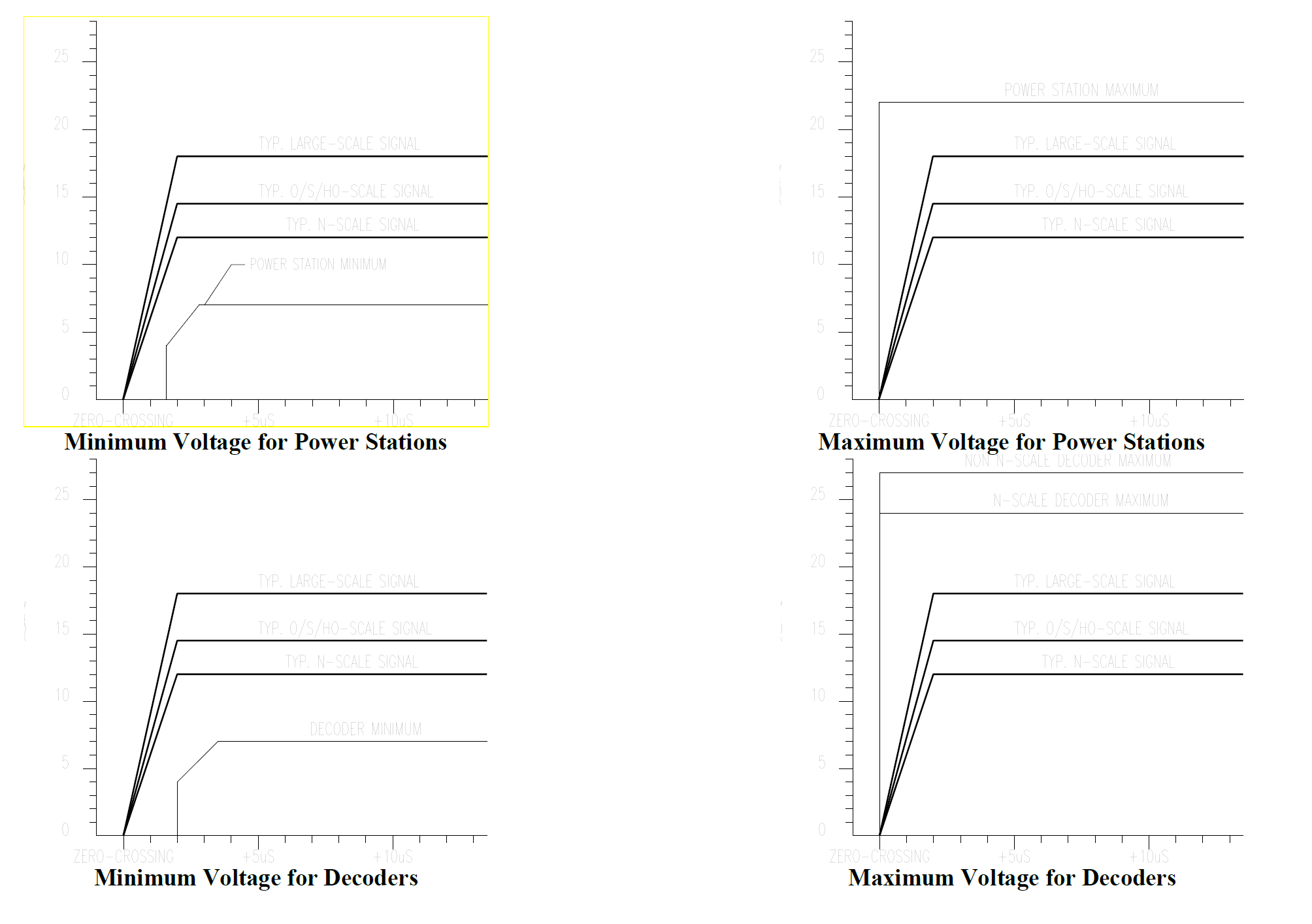
The NMRA digital signal applied to the track by any Digital Command Control system, as measured at the power station output, shall have the following characteristics, as measured under conditions ranging from no load to the maximum continuous load permitted by the power source. Transitions that cross the region between \(V_\mathrm{trL}\) and \(V_\mathrm{trH}\) [3] shall occur at the rate of \(V_\mathrm{trA}\) or faster. This signal may contain non-monotonic distortion at the zero-crossing transitions, provided that this distortion shall have an amplitude of no greater than \(\pm V_\mathrm{dist}\) [4].
Digital Decoders shall be designed to correctly decode signals with transitions whose slope is \(V_\mathrm{trRA}\) or faster across the voltage range from \(V_\mathrm{trL}\) to \(V_\mathrm{trH}\). A Digital Decoder shall correctly decode properly addressed baseline packets at a probability of \(P_\mathrm{decode}\) or higher, as defined in S-9.2, in the presence of noise (and/or other types of signals) at frequencies above \(F_\mathrm{noise}\) with a total peak-to-peak amplitude of less than (\(1 / V_\mathrm{snr}\)) of the peak-to-peak amplitude of the NMRA digital signal [5].
The exact shape of the NMRA digital signal shall be designed to minimize electromagnetic radiation such that a large layout operated using this standard can meet applicable United States Federal Communications Commission electromagnetic interference requirements [6].
Parameter |
Definition |
Min. Value |
Normal Value |
Max. Value |
Unit |
Comments |
|---|---|---|---|---|---|---|
\(V_\mathrm{trL}\) |
Transition region \(V_\mathrm{min}\) |
— |
-4 |
— |
Volt |
Low limit of bit transition region |
\(V_\mathrm{trH}\) |
Transition region \(V_\mathrm{max}\) |
— |
4 |
— |
Volt |
High limit of bit transition region |
\(V_\mathrm{trA}\) |
Transition rate |
2.4 |
— |
— |
Volt/μsec |
Transmitted bit voltage transition rate |
\(V_\mathrm{dist}\) |
Distortion amplitude |
— |
— |
2 |
Volt |
Distortion voltage during bit transition |
\(V_\mathrm{trRA}\) |
Receive transition rate |
2 |
— |
— |
Volt/μsec |
Received bit voltage transition rate |
\(P_\mathrm{decode}\) |
Decode probability |
95 |
— |
— |
Percent |
Percentage of packets decoded correctly |
\(F_\mathrm{noise}\) |
Noise frequency |
100 |
— |
— |
kHz |
Frequency of noise or other signal |
\(V_\mathrm{snr}\) |
Peak signal to noise amplitude ratio |
4:1 |
— |
— |
No units (this is a ratio) |
Peak DCC signal to peak \(F_\mathrm{noise}\) |
C: Power Transmission and Voltage Limits for Transmitting Power through the Rails
The baseline method for providing the power to operate locomotives and accessories, which shall be supported by all Digital Command Stations and Digital Decoders, is by full-wave rectification of the bipolar NMRA digital signal within the Digital Decoder [7]. In order to maintain power to the Digital Decoders, gaps in bit transmission are only allowed at specified times (see S-9.2, Section C). The peak value of NMRA digital signal, as produced by the power station and measured at the track, shall be confined to the range of \(V_\mathrm{DCCp}\) for the applicable scale, as specified in Table 3 [8]. In no case should the peak amplitude of the command control signal exceed \(V_\mathrm{DCCpmax}\) for the applicable scale.
Digital Decoders shall be designed to continuously operate in and withstand, without permanent damage to the decoder; a peak maximum voltage within the range of \(V_\mathrm{DCCr}\) as specified in table 3 for the applicable scale, measured at the track.
Scale |
Parameter |
Definition |
Min. Value |
Normal Value |
Max. Value |
Unit |
Comments |
|---|---|---|---|---|---|---|---|
N and smaller scales |
\(V_\mathrm{DCCp}\) |
Voltage limits for track for power station |
8.5 |
12 |
22 |
Volt |
Voltage produced powering the track |
HO/S/O scales |
\(V_\mathrm{DCCp}\) |
Voltage limits for track for power station |
8.5 |
15 |
22 |
Volt |
Voltage produced powering the track |
Large scales |
\(V_\mathrm{DCCp}\) |
Voltage limits for track for power station |
8.5 |
18 |
22 |
Volt |
Voltage produced powering the track |
N and smaller scales |
\(V_\mathrm{DCCr}\) |
Voltage limits for track for decoder |
7 |
12 |
24 |
Volt |
Peak voltage decoder should operate in and withstand |
HO/S/O scales |
\(V_\mathrm{DCCr}\) |
Voltage limits for track for decoder |
7 |
15 |
27 |
Volt |
Peak voltage decoder should operate in and withstand |
Large scales |
\(V_\mathrm{DCCr}\) |
Voltage limits for track for decoder |
7 |
18 |
27 |
Volt |
Peak voltage decoder should operate in and withstand |
Digital Decoders shall be designed to interpret a valid packet addressed to it whilst supplied a minimum voltage \(V_\mathrm{DCCr}\) as specified in Table 3 and to acknowledge the receipt of a command in that packet by some action. E.G. turning on a low power output to illuminate an LED. The Digital Decoder is not required to turn the motor at this voltage. This is an indication of the Digital Decoder’s ability to read valid instructions addressed to it at the specified minimum voltage at the track.
Data |
Revisions |
|---|---|
January 2019 |
Tabularized data, removing it from the text and replacing with a variable to make future revisions less prone to missing changes in the text. Cleaned up grammar and language. |
February 2019 |
Table 3 increased large-scale power station maximum voltage large to 24v from 22v. |
July-August 2019 |
Text related to Table 3 to clarify the decoder must operate continuously in the maximum voltage specified without sustaining permanent damage. The decoder must read and acknowledge a valid instruction addressed to it at the minimum voltage specified. |
Footnotes